Scanning Probe Microscopy (SPM) comprises many techniques reflecting interaction of a tip with investigated surface and providing information about the surface’s topography, magnetic, electric and elastic properties The Scanning Tunneling Microscopy (STM) and Atomic Force Microscopy (AFM) were the first invented scanning microscopes.
The basic principle of STM is that the tunneling current between a conductive tip and a sample is exponentially dependent on their distance. As the tip scans the sample’s surface, it encounters sample features of different heights, resulting in an exponential change in the tunneling current. A feedback loop is used to maintain a constant tunneling current during scanning by vertically moving the scanner at each (x,y) data point until a “setpoint” current is reached. This technique is typically limited to conductive and semiconducting surfaces.
In case of soft biological materials and polymers Atomic Force Microscopy (AFM) turned out to be more appropriate. During scanning the tip experiences interactions originating from ionic repulsion, van der Waals, capillary, electrostatic and magnetic forces, or elastic and plastic deformations.
There are 3 primary modes of AFM:
- Contact Mode (The main interacting forces between the tip and the surface are very short range repulsive forces)
- Tapping Mode (Cantilever oscillates over the sample’s surface at a frequency close to its resonance frequency)
- Non-Contact Mode (For nondestructive analysis, but with worse resolution)
AFM can provide information about following surface properties: friction and adhesion forces, viscoelastic properties, Young modulus (Lateral Force Microscopy , Force Modulation Microscopy, Phase Detection Microscopy), magnetic structure (MFM), electrostatic properties (EFM), electric properties: current distribution (Conductive AFM), carrier density or dopant concentration (ang. SCM).
Any kind of samples can be analyzed: polymers, adsorbed molecules, films, fibres, powders, in air, in controlled atmosphere or in liquid medium.
Application:
- metals: tooling studies, roughness measurements, corrosion studies...
- solid powder catalysts: aggregate structural determination,
- polymers: determination of morphology and surface properties, kinetic studies, aging phenomena, surface treatment modifications, adhesion force measurement and indentation,
- biological samples, biomaterials: macromolecules association and conformation studies, adsorption, kinetic of molecules on polymer surfaces, nano- and microparticle structures, Langmuir-Blodgett, film studies.
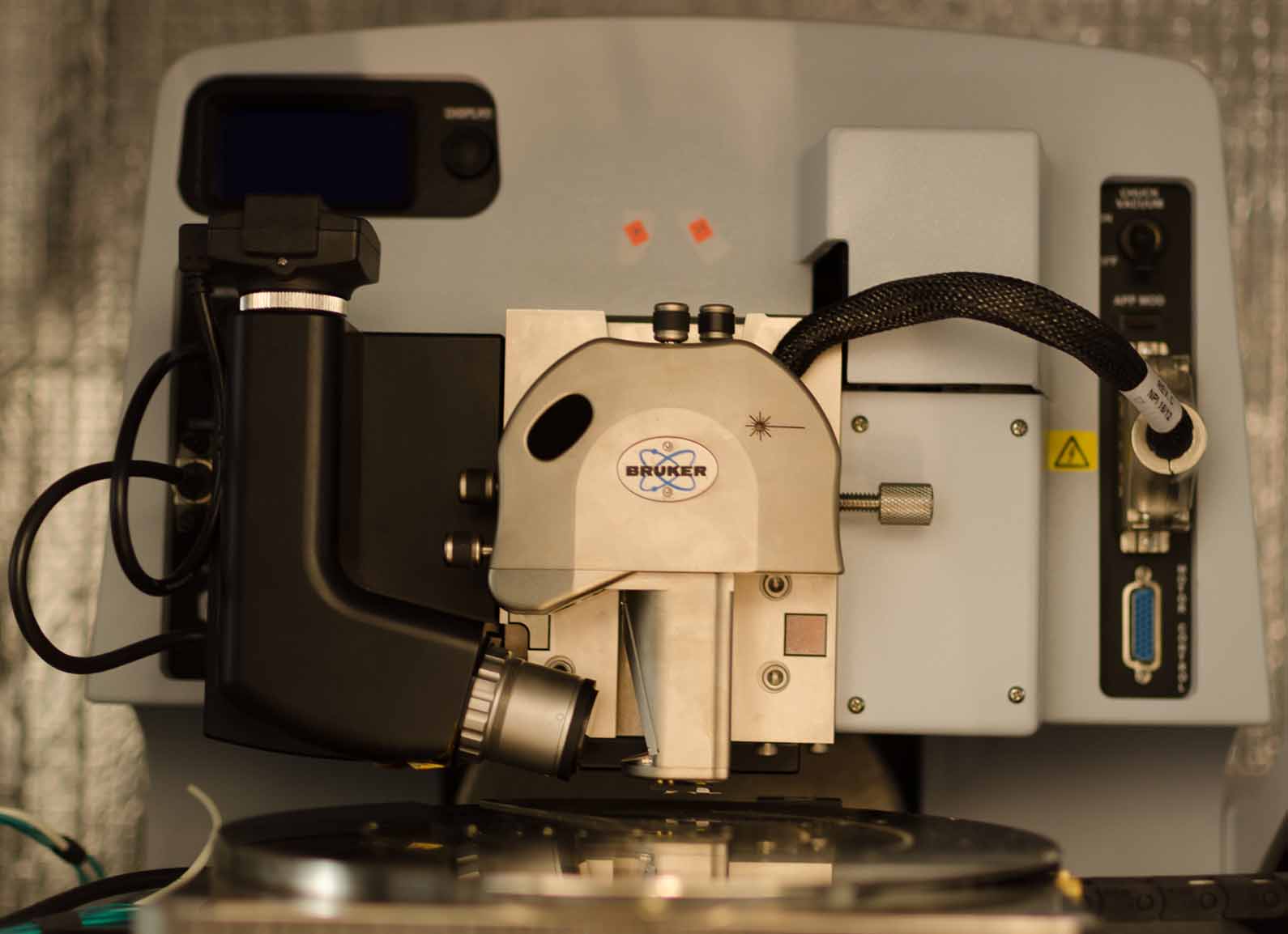
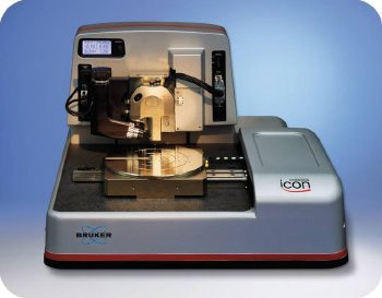
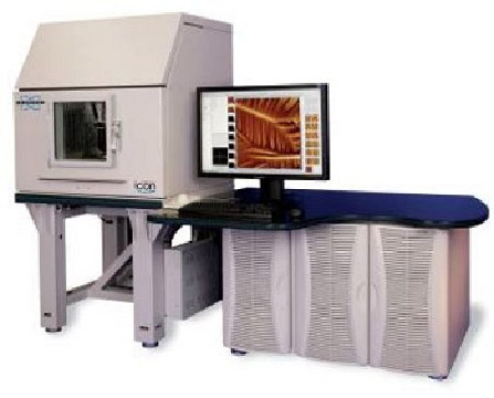
Bruker’s Dimension Icon Atomic Force Microscope
Available modes: ScanAsyst (air/liquid), Tapping Mode (air/liquid), Contact Mode (air/liquid), Lateral Force Microscopy, PhaseImaging, Lift Mode, MFM, Force Spectroscopy, PeakForce Tuna, Force Volume, EFM, Surface Potential, Piezoresponse Microscopy, Force Spectroscopy, PeakForce QNM.
Examples:

Topography of Ni islands on the Si substrate
 (b)
(b)
Topography (a) and DMT Modulus (b) of lamellars domains in PEO


Topography and friction properties of mica layer
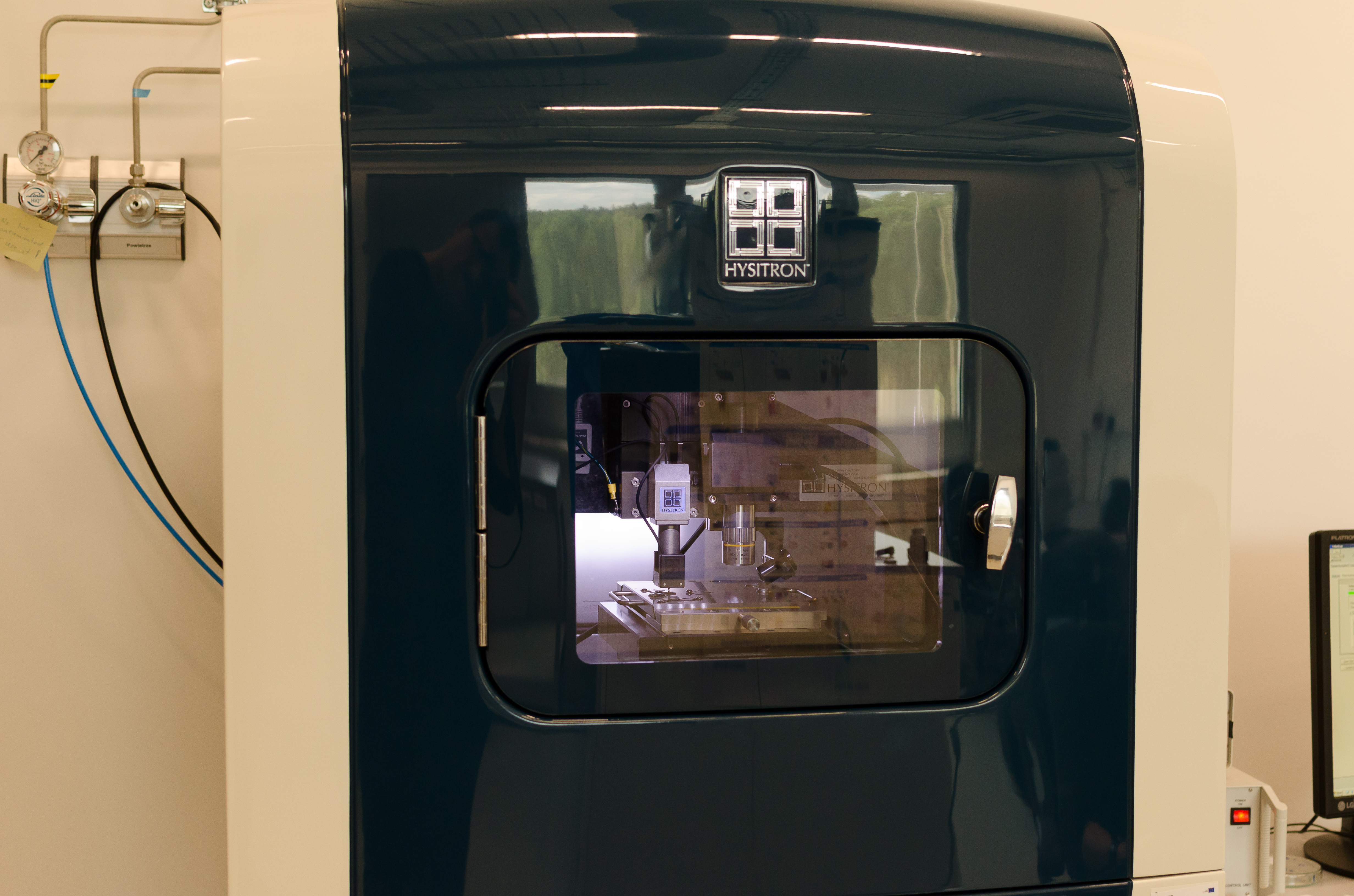
Nanoindenter
The nanoindenter is a low load nanomechanical test system for measuring the hardness and elastic modulus of thin films and coatings. Presented in picture 1 the Hysitron TriboIndenter 950 provides quantitative information about nanomechanical properties of samples such as: Young modulus, energy loss, hardness, fracture toughness, scratch resistance, critical delamination forces, and friction coefficients and other mechanical properties via nanoindentation.
The transducer technology provides X, Y, Z and Z piezo positioning. TriboIndenter provides testing based on quantitative, controlled nanoindentation of surfaces. Automated precision testing, staging and sample positioning allows maximum throughput of samples.
Optional functions as Young modulus mapping over a surface of a sample and SPM imaging are its advantage. Resolution of the surface imaging before and after nanoindentation is of order of 10 nm.
Key parameters:
- XY scan range 240 x 120 mm,
- Z scan range 40 mm,
- resolution 700 nm,
- normal shift 5 um,
- resolution of the normal shift 0,02 nm,
- Noise Floor 0,2 nm,
- measurements in air and fluid environment,