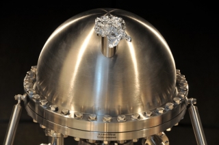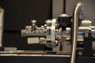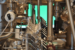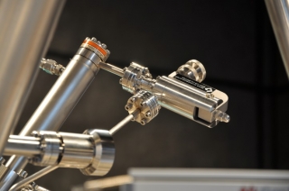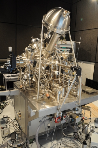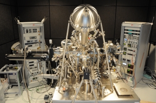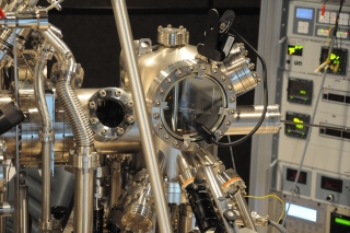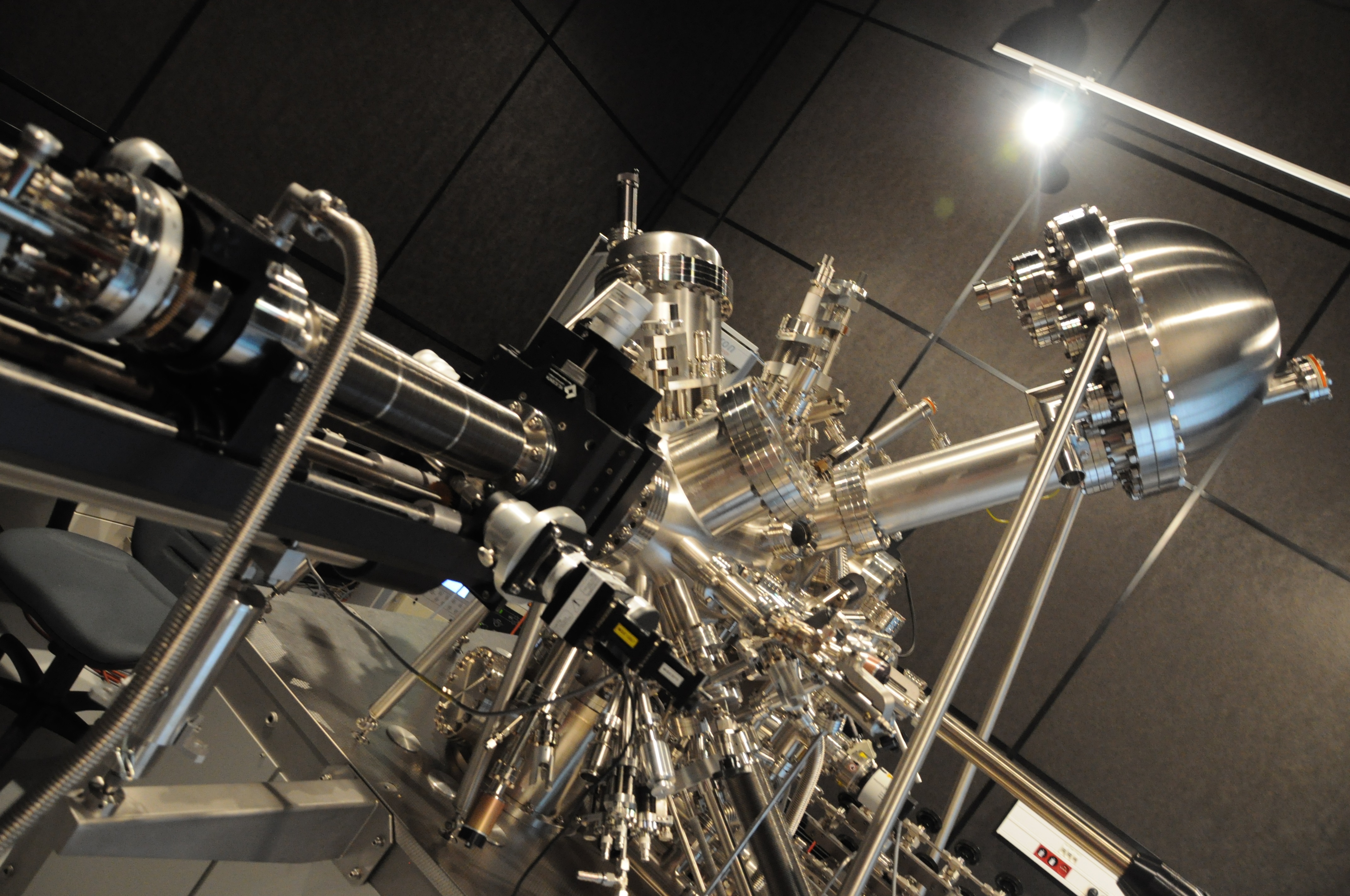
Omicron Nanotechnology dual chamber multiprobe surface science system for in-situ preparation, modification and detailed analysis of various nanostructures and thin films in the ultra high vacuum (UHV) conditions.
Two main experimental techniques:
- Electron Spectroscopy for Chemical Analysis (ESCA) for determination of the chemical composition of the sample,
- Scanning Probe Microscopy (SPM) for measuring and imaging of the various surface properties with atomic resolution.
General features:
- two interconnected chambers: first comprising the surface preparation units and ESCA, while the second one dedicated to support SPM techniques
- multistage pumping system for acquiring the pressure of the order of 10-11 mbar inside both chambers
- fast entry lock for quick sample and SPM sensors exchange
- 5-degrees-of-freedom Omniax manipulator with cooling and heating stages for sample preparation, transfer and ESCA measurements
Variable Temperature Scanning Probe Microscope (VT SPM)
- Scanning Tunneling Microscopy/Spectroscopy (STM/S) with sub-pA current operation
- beam deflection Atomic Force Microscopy (AFM) for contact and non-contact measurements with the possibility to operate in various modes depending on the cantilever used (e.g. high resolution AFM, Electrostatic Force Microscopy – EFM, Scanning Kelvin Probe Force Microscopy – SKPFM and Magnetic Force Microscopy – MFM)
- Q-Plus sensor combining AFM and STM
- Matrix Control System
- temperature control in the range of 30 ÷ 500 K
- tip preparation tool for the in-situ conditioning of the STM tips
ESCA
- multipurpose hemispherical energy analyzer SPHERA II
- XPS with dual anode X-ray source (DAR 400) and monochromatic X-ray source (XM 1000)
- UPS high intensity VUV source (HIS13)
- AES electron source for 0.1 - 5 keV beam energies and spot size 300 mm (EKF 300)
- electron source for charge neutralisation (CN 10)
Preparation chamber
- Single and Triple Electron Beam Evaporators (EFM 3 & EFM 3T), Organic Material Effusion Cell (OME40) and Low Temperature Effusion Cell (NTEZ) for the clean deposition of various atoms and molecules. Possibility of the controlled sub-mono-layer and multi-layer thin film growth with the use of Film Thickness Monitor (FTM)
- atomic gas sources: Atomic Hydrogen Source (EFM-H) for passivation and Oxygen Atom Beam Source (OBS40) for controlled oxidation of the sample surface
- Cold Cathode Sputter Ion Source (ISE5) for sample cleaning, depth profiling with ESCA and controlled induction of defects
- Quadrupole Mass Analyzer (Quad 300) for residual gas analysis (vacuum purity and leak detection)
 Surface profile Si (111) 7x7 along the marked line
 Si surface (111) 7x7 imaged on two different voltage polarizations between the blade and the sample

STM. Surface Si (111), reconstruction 7x7, obtained by high-temperature processing in ultra-high vacuum (flash). Atomic resolution.


