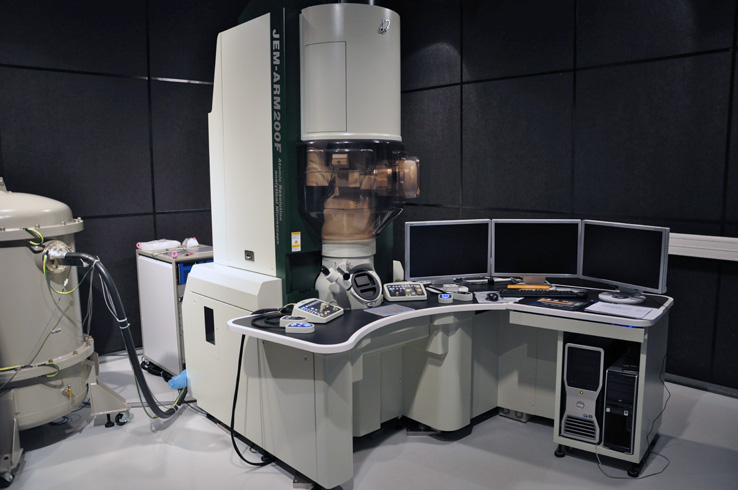
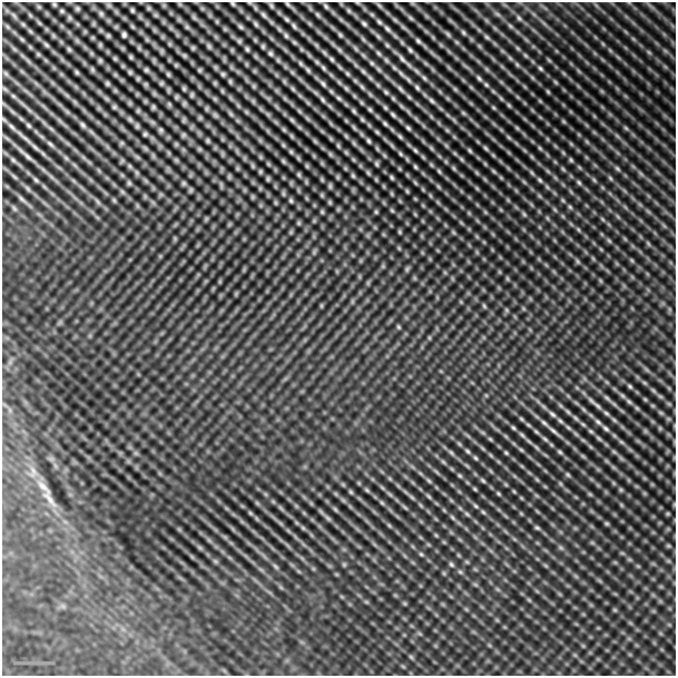
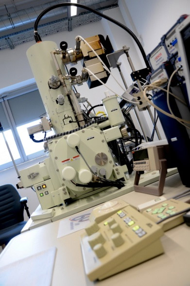
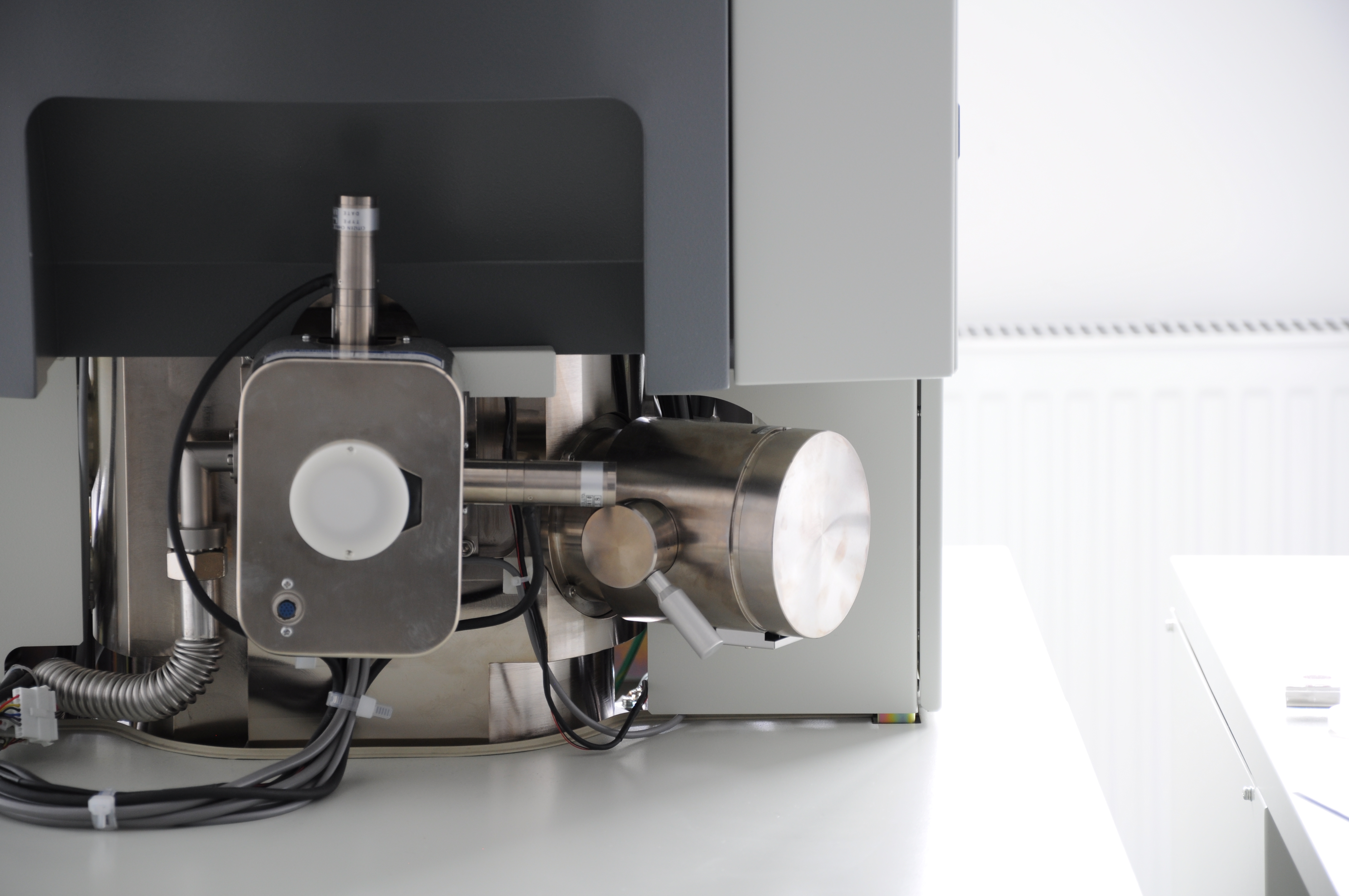
High Resolution Transmission Electron Microscope HRTEM Jeol ARM 200F
Specification:
- Maximum accelerating voltage: 200 kV
- Maximum resolution: 0.63 Å
- STEM
- Detectors: Bright, Dark Field Detector, High-Angle Annular Dark Field Detector
- Spectroscopy: Energy Dispersive X-Ray Spectroscopy (EDS), Electron Energy-Loss, Spectroscopy (EELS), Gatan Imaging Filter
Applications:
- High resolution microscopy of nanostructures (nanotubes, nanospheres)
- High resolution microscopy of semiconductors
- Elemental analysis
- Electron diffraction
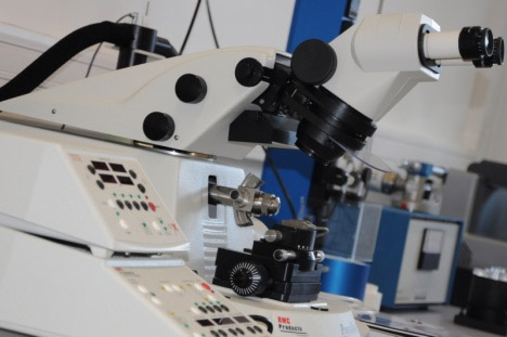
Transmission Electron Microscope Jeol 1400
Specification:
Maximum accelerating voltage: 120 kV
Maximum resolution: 0.2 nm
Holder for cryoTEM
Applications:
Imaging of nanosystems
Studies of soft matter (polymers, colloids) and biological systems
Electron tomography and 3D imaging
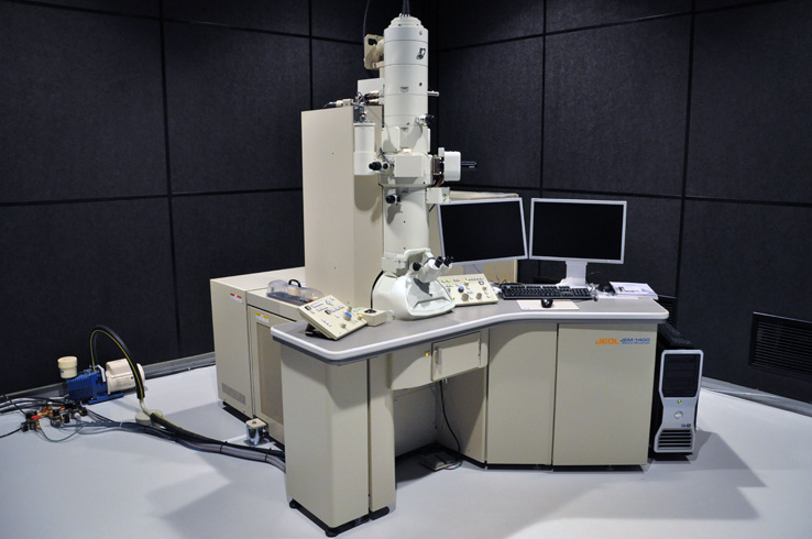

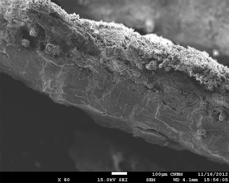
Scanning Electron Microscope SEM Jeol 7001TTLS
Specification:
- Maximum accelerating voltage: 30 kV
- Maximum resolution: 1.5 nm
- cryoSEM
- Spectroscopy: Energy Dispersive X-Ray Spectroscopy (EDS)
- Electron beam lithography
Applications:
- Imaging of nanosystems
- Studies of soft matter (polymers, colloids) and biological systems
- Studies of porous systems
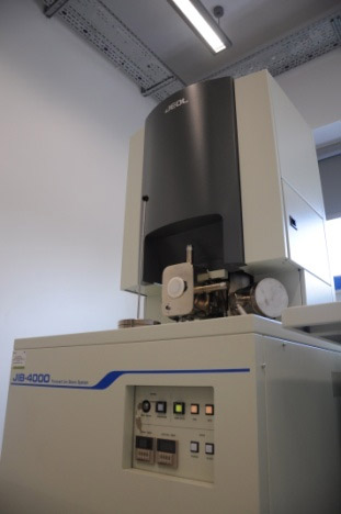
Focused Ion Beam – FIB
Specification:
Ion source: Ga liquid metal ion source
Maximum resolution of image: 5 nm
Maximum current beam: 60 nA at 30 kV
Applications:
Sample preparation for TEM and SEM
Litography
Equipement for sample preparation
- Critical point dryer
- CryoPlunge for deep and rapid freezing
- Ultramicrotome (cryo option)
- High vacuum coating system