Supervisory institution:
National Science Centre
Project manager:
Dr. Karol Załęski
Budget:
785 600,00 PLN
The amount of digital information in the world increases every day. The emergence of wireless technologies, smart products and software-defined business are playing a major role in catapulting the volume of the world’s data. The digital universe is doubling in size every two years and will reach about 50 trillion gigabytes (GB) in 2020. For perspective, the stack of standard 128 GB tablets containing this amount of information would reach the way to the moon 5 times [1]. Hence, there is a need for computing devices that can operate with small energy consumption.
In conventional electronics the information is carried by the charge of the electrons. The electric current cause Joule heating and high energy dissipation. In spintronics devices, in which spin-polarized currents play a key role, information is carried by the electron spin rather than charge and is thus free of ohmic energy dissipation. It allows for substantial reduction of the power consumption in digital data processing [2]. So far spintronics materials have found application mostly in the read heads for magnetic disk drives or magnetic random access memory (MRAM). The listed above devices are manufactured by such leading brands as IBM, Hitachi, Samsung and many others. The next challenge is to exploit the field of spintronics to execute logic processes [3].
Two-dimensional (2D) crystal such as graphene has demonstrated potential for high-performance spintronics [4,5]. In particular, combination of high-carrier velocity and a long spin lifetime makes graphene a very promising spin channel material [5]. In graphene-based spintronic devices the spin current flows from spin injector, where the spin-polarized current is injected into graphene, to spin detector where the current is detected. The magnitude of the signal measured in the device – the device performance – is dependent on the spin polarization of the electrodes, the spin-conductance mismatch between spin channel and the electrodes and the interface quality, among others.
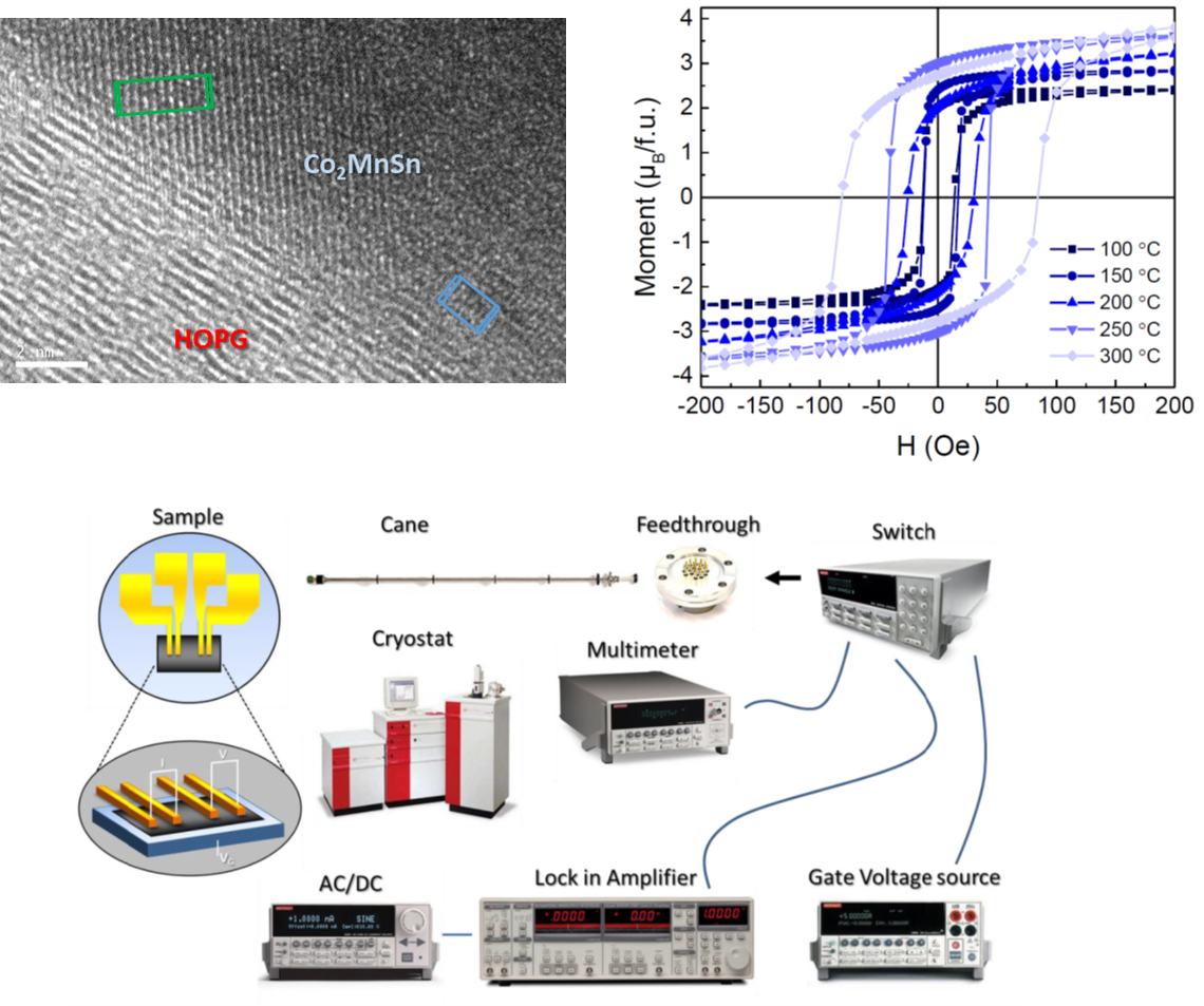
The scientific problem aimed to be solved by the proposed project is to improve the spin injection and detection efficiency in the graphene-based spintronic devices. For this purpose, half-metallic and spin-gapless semiconductors Heusler alloys will be used as a material for the electrodes in graphene-based lateral spin-valve devices. Half-metallic (HM) materials present metallic behaviour in one spin channel and semiconducting behaviour in the other one. This type of the electronic structure results in full spin polarization of the Fermi level (conducting) electrons. In the case of the spin-gapless semiconductors (SGS) there is a zero gap at the Fermi level in the majority spin channel and the finite (semiconductor-like) gap in the minority spin channel. Because of the almost vanishing zero-width band-gap the mobility of carriers is stronger than in usual semiconductors. Since graphene can be considered as a gapless semiconductor one can anticipate enhancement of the spin polarization degree the electrons injected from SGS contact to graphene spin channel.
The pioneering idea presented in the project – the use of contact electrodes made from HM or SGS Heusler alloys in LSV devices – will highly impact on the development of the graphene spintronics field. The direct growth of the Heusler alloys contact electrodes on graphene channel should improve the properties of LSV devices.
[1] emc.com/about/news/press/2014/20140409-01.htm
[2] J. Atulasimha, S. Bandyopadhyay, Nanomagnetic and spintronic devices for energy-efficient memory and computing, Wiley (2016)
[3] C. Felser, G.H. Fecher, Spintronics: From Materials to Devices, Springer (2013)
[4] M.V. Kamalakar, et al., Long distance spin communication in chemical vapour deposited graphene, Nat. Commun. 6 6766 (2015)
[5] W. Han, et al., Graphene spintronics, Nat. Nanotechnol. 9 794 (2014)


